
Printed Circuit Boards (PCBs) are an essential part of modern electronics. They are used in everything from smartphones and laptops to cars and home appliances. PCBs are an efficient way to connect components, and transmit signals and power between them. However, designing PCBs is not always an easy task. Design errors often occur, which can be costly and time-consuming to fix, especially for beginners with little experience. In this article, let’s discuss the 5 most common PCB design errors that inexperienced people often make and how to fix them. These errors can lead to signal interference problems, thermal problems, power supply problems, and even component damage. By avoiding these errors, you can ensure the performance and reliability of your board.
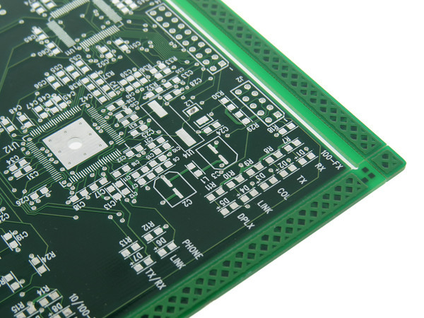
Design Error 1: Not using a Ground plane
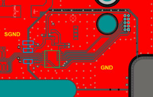
Figure 1: Ground plane on printed circuit board
A ground plane is a large copper area on the PCB that is connected to ground. It acts as a shield, preventing electromagnetic interference (EMI) from affecting the signal on the PCB. Not using a ground plane can lead to unwanted noise in the signal, which can affect the performance of the circuit.
To fix this, you should add a ground plane to your PCB design. Most PCB design software has a built-in feature that allows you to easily add a ground plane. Simply create a new layer in your design and connect it to the ground grid. This will create a large copper area that can be used as a ground plane.
Design Error 2: Not checking for Clearance constraints
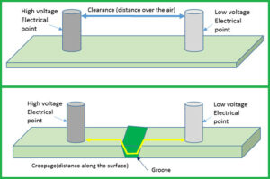
Figure 2. Comparison of Clearance and Creepage definitions
Clearance Rule (DRC) refers to the minimum distance between two conductive objects on the PCB, such as two tracks or a track and a solder pad. Failure to check the clearance rule can lead to short circuits or signal interference.
To fix this error, you should check the clearance rule in your PCB design software. Most PCB design software has a feature that allows you to set clearance rules for different objects on the PCB. These rules will prevent objects from being placed too close together and causing short circuits or signal interference. Besides, these factors are also limited by the factory’s production capacity. If these minimum clearance parameters exceed the factory’s production capacity, it will affect the fabrication ability of the board.
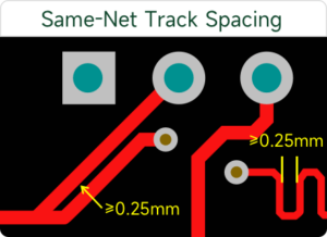
Figure 3. Each manufacturer has different minimum spacing limits that you need to consider when designing.
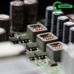
Design Error 3: Not using power filter capacitors
A power filter capacitor is a capacitor placed between the power and ground pins of an integrated circuit (IC). It helps stabilize the power supply and prevent noise on the power line. Not using a power filter capacitor can result in unstable power supply and reduced circuit performance.
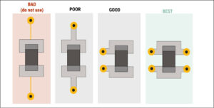
Figure 4. How to design the location of the power filter capacitor (SMD type)
To fix this, you should add a filter capacitor to your PCB design. The size and type of filter capacitor will depend on the IC and the supply voltage. It is important to consult the IC datasheet to determine the appropriate capacitor value and placement.
Design Mistake 4: Not Labeling Components
Not labeling components can lead to confusion and errors during the soldering and assembly of the board. If not labeled properly, it is easy to confuse the location and orientation of components, especially in complex designs with high component density.
To overcome this error, you should label all components in your PCB design. Most PCB design software has a feature that allows you to add labels and symbols to the location of components. It is important to clearly display the name and orientation characters to avoid confusion.
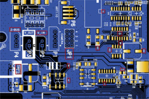
Figure 5. Add labels and symbols to components in the circuit
Design Error 5: Not running Design Rules Check (DRC)
DRC is a feature of your PCB design software that checks your PCB design for errors, such as minimum clearance distances, overlapping objects, and unconnected pins. Failure to run DRC can result in errors in your PCB design, which can cause problems during assembly or affect the operation of your PCB.
To fix this, you should run DRC in your PCB design software. Most PCB design software has a built-in DRC feature that checks your design for errors and provides a report of any issues found. It is important to set up design rules that are required by your design, combined with manufacturer rules to ensure manufacturability and project requirements are met.
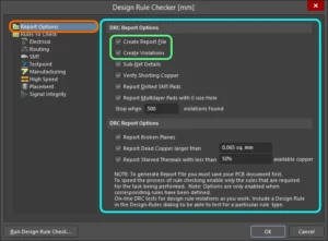
Figure 6. Always check design parameter constraints to avoid errors on the circuit
Conclusion
Designing PCB layouts is a challenging task, especially for those who are new to the field. Hopefully, through this article, you can understand the 5 common mistakes that often occur when designing circuits.
By overcoming these mistakes, you can avoid common problems such as signal interference, power supply problems, and component damage. This will help save time and costs when processing circuits. Currently, most PCB design software has built-in features that help you easily add components, as well as check design rules to avoid the above errors. In addition, always check the production capacity as well as consult the manufacturer’s advice to help you minimize errors on the board.


 Tiếng Việt