
Reflow soldering is one of the popular techniques in SMT soldering on PCBs. This method has advantages such as: precise component placement, uniform solder quality and high production efficiency… However, like many other soldering processes, reflow soldering also has its own advantages and disadvantages. Let’s discuss with Hatakey Electronics some common problems that arise during SMT soldering using the reflow soldering method and solutions to these problems. Through this article, we hope to help SMT technicians find appropriate solutions to minimize errors and increase processing quality.
1. Solder Bridge
One of the most common errors is the Solder Bridge phenomenon (Figure 1). This phenomenon occurs when an unwanted bond of solder is formed between two circuit traces, solder pads, or component pins to form a conductive path. Especially as printed circuit boards become smaller with higher component density, bridging errors are more likely to form.
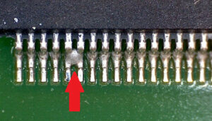
Figure 1: Bridged solder joints between IC pins
Some causes of bridged solder joints include:
- No coating or ink separating the solder pads close together
- The distance between the solder pads, component pins is too close
- The solder paste layer on the solder pad is too thick, too much
- Residue accumulated on the surface of the circuit board or stencil printing mold
- Errors in the process of printing the paste (the printed paste is misaligned) or placing the components
- Insufficient preheating temperature
Bridged solder joints cause short circuits that damage the circuit board during use. Therefore, limiting and detecting these errors early in the SMT processing is extremely important to save costs as well as time to repair faulty circuits.
How to Fix
The best way to solve bridging errors is to prevent them from happening in the first place. Many of these are due to design or soldering process issues. If a bridging error occurs on one board, it is more likely to occur on other boards.
- Coating. Coating between adjacent solder pads is an important component in preventing bridging errors from forming. The color of the coating also plays a significant role in detecting solder errors. There are many options for board coatings for aesthetic purposes, but green has the highest contrast and lowest cost, making it effective in detecting solder errors before they become a problem.
- Optimize the design: Miniaturization is an important factor in efficient PCB design. Unfortunately, designs where the solder pads and stencil die holes are too close together can result in solder bridges. Following PCB design and layout standards can help you avoid this costly mistake.
- Adjust the amount of solder paste. Bridging errors often occur when there is too much solder paste on the solder pad. Adjusting the solder paste pressure or applying too much force when picking up components can force the solder paste off the solder pad, creating solder bridging errors. Also, make sure that the solder paste and flux used are suitable for the soldering process, and are of good quality.
- Clean the Stencil. If the stencil is not cleaned properly, residue can build up and lead to bridging errors in subsequent prints. Make sure the stencil is always clean before processing to ensure the error rate is minimized.
2. Tombstone faults
Tombstone is a phenomenon of component being channeled during SMT processing in which the component is completely erected like a tombstone or partially erected. This fault affects the connection as well as the function of the board.
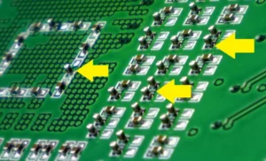
Figure 2. Tombstone error on the PCB board
The main cause of this phenomenon is that the tension holding the two ends of the component during the soldering process is not balanced, leading to one end being lifted up. Some factors that contribute to this phenomenon include:
- The process of setting the temperature profile for the soldering furnace (Thermal Profile) is not optimized. When the process of setting the temperature of the furnace is not optimized, the slope of the heat curve is too large, leading to the temperature in the furnace changing rapidly between the heat-generating areas. This can easily lead to the solder paste on one component leg melting faster than the other leg.
- The amount of tin between the component soldering pads is not uniform. The difference in tin between the soldering pads can also easily lead to the component being lifted on the side with less solder paste during the oven process.
- Incorrect component library. Incorrect design of the component soldering pad leads to one side of the pad being larger than the other, or placing a via in one side of the soldering pad can also cause the phenomenon of foot lifting.
- Misalignment during component placement. Misalignment of components during component placement can also cause the component to be out of alignment on the side that has less contact with the solder pad during the furnace process.
- Errors from circuit boards and components. The quality of PCB boards and input components for the production line is also one of the causes of this phenomenon. Oxidation of solder pads or component pins leading to lack of tin can lead to component out of alignment during processing.
How to fix
- Adjust the oven’s heat profile appropriately. It is necessary to pay attention to the heat output rate and intensity of the ramp-up, “soak” (soak) circuit in heat and cool during the convection soldering cycle. This helps ensure that the PCB is heated evenly and minimizes the temperature difference between the PCB areas
- Optimize the design such as designing the correct solder pad, wiring, placing vias or distributing components on the circuit.
- Check the quality of solder paste printing with SPI (Solder Paste Inspection) machine. Checking the quality of solder paste printing helps ensure that errors and inconsistencies are detected during the solder paste printing process, helping to detect early and separate substandard printed circuit boards.
- Ensure accuracy during component placement. Setting the component placement mode also plays an important role in minimizing errors during the processing. In addition, AOI inspection machines can be arranged to detect errors during the installation process.
- Control the quality of input materials. Preserving and checking the quality of components as well as PCB printed circuits before processing is an indispensable part to avoid the situation of materials being oxidized, damp, … which can easily lead to the situation of not absorbing tin when soldering.
3. Solder Ball Defect
Solder ball is the most common defect in SMT processing. A solder ball within 0.13mm of the circuit line violates the minimum conductive distance on the PCB. According to IPC A 610 standard, a PCB is considered defective when there are 5 solder balls within 600 mm2. This defect can cause short circuits, or reduce the quality of the solder joint.
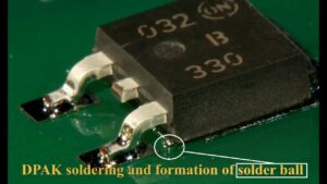
Figure 3. Solder Ball Failure
Some of the main causes of this phenomenon include:
- Moisture in the PCB. Storing the PCB in an improper humidity environment or not drying it before processing can cause solder balling during the soldering process.
Incorrect melting temperature can cause the solder paste to melt too quickly or not solidify completely, leading to the formation of solder balls. - Activity of the solder paste. The solder paste plays an important role in reducing oxides on the solder surface. However, if the solder flux is too active or not sticky enough, it can cause the molten solder to separate and form individual balls.
- Oxidation of solder particles. Oxidation on the surface of the solder particles can hinder adhesion during melting, causing solder balls to form. Proper storage and handling of the solder paste can help minimize oxidation.
- Errors in the solder paste printing process or due to the stencil being not cleaned properly, causing the solder paste to stick to unwanted locations on the PCB surface.
Solution:
- Reheat/rebake the PCB board before SMT processing
- Adjust the oven temperature configuration accordingly
- Clean the stencil before processing
- Use a good quality tin paste suitable for the processing process.
4. Solder voids
Voids are air pockets or gas-filled spaces that develop within a solder joint after the fabrication process. They can negatively impact the electrical and thermal conductivity of the solder joint, leading to reduced reliability and increased failure of the board. Voids can occur in solder joints, but are most common when soldering ball-edge gate assembly (BGA) and QFN components.
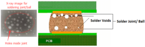
Figure 4. Porosity in solder joints
Common causes of porosity include:
- Outgassing. Gases produced during the melting of solder paste can become trapped inside the solder joint. This can occur if the gas cannot escape due to insufficient venting or the viscosity of the solder paste is too high.
- Oxidation: The presence of oxide layers on component pins, pads or solder balls can interfere with the wetting and adhesion of the solder. This creates voids within the solder joint.
- Improper handling and storage of solder paste, such as exposure to environments with high temperature and humidity fluctuations, can cause changes in the viscosity and consistency of the solder paste, leading to porosity. Ensuring that the solder paste is stored according to the manufacturer’s instructions can help reduce porosity.
Solution:
- Optimize the heat profile of the soldering oven: Adjust the heat profile of the convection oven to gradually increase the temperature and ensure enough time at the melting points of the solder to allow the gas to escape more effectively, reducing the possibility of void formation.
- Choose the right solder paste. Choosing a solder paste with low porosity properties, or a solder paste with the right flux composition, can help minimize voids.
- Control the stencil frame design and the paste printing process. Ensure the appropriate mold design such as the size and shape of the holes corresponding to the component solder pads. Strictly control the solder paste printing process on the board surface, ensuring the amount of printed paste is uniform and accurate, also contributing to minimizing the possibility of voids in the solder joint.
- Store the input components and PCBs in a suitable environment. Ensure that the components and PCBs are free of dirt or oxidation that reduces the wettability of the solder paste.
5. Head in Pillow (HIP) Error
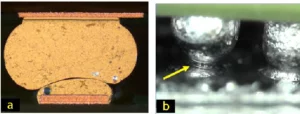
Figure 5. Examples of HIP defects. a) Optical cross-section of a solder joint. b) External view of a BGA component solder joint
This phenomenon occurs when the solder balls (usually the ball legs of BGA components) and the solder paste on the solder pad of the circuit board are melted but do not fuse together. The cross-sectional image (Figure 5a) clearly shows the boundary between the solder balls on the BGA component and the solder paste on the circuit board, quite similar to the pillow image.
The causes of HIP errors can be:
Surface oxidation, or poor wetting ability of the solder paste.
- Components and circuit boards are warped under the effect of heat, especially when processed with lead-free tin at high temperatures, causing the solder balls of the components to lift off the solder paste layer.
Solder paste quality. The solder flux helps promote the wetting process of the solder joint by removing the oxidation layer on the surface. If the flux in the solder paste is not enough, this process can be hindered. - Lack of solder paste also causes the solder balls on the BGA to not contact the solder paste layer on the component solder pad, causing HIP phenomenon
- Inappropriate oven temperature configuration causes the solder paste to melt before the solder balls melt to combine, or insufficient temperature prevents the process of wetting the solder balls on the components.
Solution:
- Optimize the oven temperature configuration to match the characteristics of the components and solder paste. Pay attention to reducing the peak convection soldering temperature or adjust the temperature to increase on the bottom side.
- Ensure that the components and the board surface are not oxidized.
- Adjust the design of the stencil solder mask frame, speed, and pressure of the sweeper to ensure the amount of solder paste printed.
- Use the right type of solder paste with the right flux.
Conclusion:
The above are five common SMT errors in the processing process using a convection soldering oven. Although there are many advantages, the convection soldering method still has its own problems that we need to pay attention to. In general, optimizing the temperature configuration of the oven, the quality of the solder paste printing process, the accuracy of component placement, and the design of the circuit board… all affect the quality of the soldering process. In addition, applying modern automatic monitoring equipment such as AOI, SPI, X-ray machines… to control the quality of each step in the process plays an extremely important role in quality control.
Soldering errors are a common problem in SMT processing and often have serious consequences in terms of time and money. Finding a reliable assembly unit to ensure that SMT errors on finished circuit boards are minimized is extremely important. Currently, Hatakey Electronics is providing high-quality PCBA circuit board assembly services. With many years of experience in the PCBA field as well as a modern equipment system, we are confident in bringing customers the best quality processed products and the most competitive prices on the market.
Contact us today for advice and quotes!


 Tiếng Việt