
What is Hot Air Solder Leveling (HASL)?
Hot Air Solder Leveling (HASL) is a hot air leveling or tin plating process that involves coating the exposed copper surface with a layer of tin alloy to prevent oxidation and provide a good solder surface for subsequent soldering assembly. The basic process of HASL is to quickly immerse the printed circuit board into a high-temperature liquid tin bath. Through the action of flux and high-temperature liquid tin, a tin-copper alloy (IMG) is formed. Then, using a circuit clamp, the circuit board is lifted out of the tin bath. At this time, high-pressure hot air will blow away excess tin from non-copper points and completely flatten the surface of the circuit board.
Copper Peeling Error During HASL
The HASL process provides us with better circuit processing and increased durability for PCB circuits. However, in the actual HASL process, copper peeling does occur. In single-sided PCBs, this phenomenon most commonly occurs in plated through-holes. In double-sided PCBs, it occurs in narrow annular through-hole solder pads, especially with long holes. This copper stripping phenomenon (Figure 1) can be caused by the following main reasons:
- The HASL bath temperature is 275-300°C, which is far above the glass transition temperature of the board (TG Point). When subjected to high temperatures and high pressure gas, the circuit may have copper stripping or warping. Without the support of large surface solder pads, the copper in the through-hole will peel off the hole wall.
- During the HASL process, copper and tin combine to form a copper-tin alloy. This compound can corrode some copper segments. This reduces the adhesion of the circuit board surface.
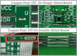
Figure 1: Faults on single-sided and double-sided PCBs.
Protection Methods
To illustrate, let’s use the analogy of climbing a cliff (Figure 2). If both hands grip the protruding part of the cliff with a larger grip area, climbing will be easier. Similarly, the copper surface inside the via holes has a similar behavior. When both the top and bottom layers have solder pads, the tin adhesion will be stronger. In this case, the phenomenon of copper peeling will be reduced. When only one layer has a solder pad, the tin adhesion will be reduced. For single-sided or double-sided PCBs with small ring solder pads, consider switching to double-sided PCBs with ring sizes of 0.3 mm or larger.
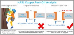
Figure 2: Visual comparison example.
If switching to a double-sided PCB is not feasible due to insufficient clearance between the via holes or other reasons, consider using the ENIG (gold-plated) method. Gold-plated solder pads have a smoother surface and are suitable for BGA boards. For cases where copper is not desired in the hole wall, choose a non-copper-plated via hole. If a connection between both sides is required, use the via hole on the side of the solder pad. Especially for high-current applications, make sure to add enough via holes.
Conclusion
So we have learned the copper protection method when using HASL for PCB circuits. If you have any difficulties, please contact us. With a team of technicians with many years of experience in the industry at our company HATAKEY Electronics.
Hatakey.com.vn Electronics Company specializes in providing services related to PCB circuit boards with many different sizes and colors. In order to meet the increasing needs of customers. Currently, our company is offering a preferential program to our customers. Specifically, when customers order printed circuit boards with a maximum quantity of 10 circuits (size smaller than 10x10cm), they will enjoy the best price policy on the market with only 89,000 VND. Thank you for taking the time to read the article.
Some related articles here.
For more information, please contact:
Sales 01: 0965 833 553
Email 01: hatakeyvn@gmail.com
Sales 02: 0927 277 222
Email 02: sales.hatakeyvn@gmail.com
Service feedback: 0971 687 227


 Tiếng Việt