
Printed Circuit Boards (PCBs) are the backbone of most modern electronic devices. They provide the foundation for connecting electronic devices. For beginners, PCB design may seem complicated, but with the right approach, it becomes an easier task and brings great benefits. This article will guide you step by step through the PCB design process in EasyEDA software, from planning to final testing.
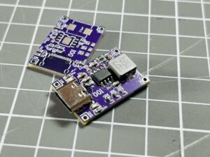
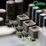
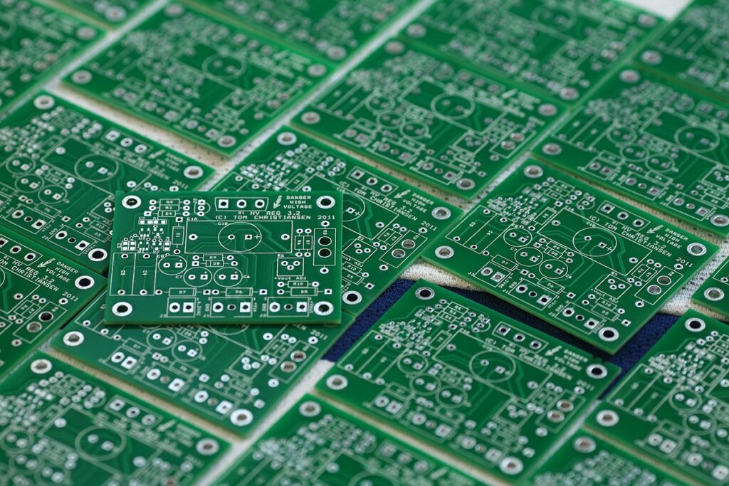
Figure 1 Finished PCB after soldering components
Now, let’s look at the process of designing a lithium-ion battery charging module as an example. TP4056 is one of the most popular charging modules today, so it would be great to create version 2 of the famous TP4056 charging module. But to increase the current rating, we replaced the circuit with a new IC called IP2312, keeping the same PCB shape as TP4056. It is capable of handling loads up to 3A. Continue reading to get detailed instructions.
1. PCB Design Steps
Step 1: Understand the requirements of the circuit
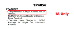
Figure 2. Understand the requirements, features, and operating principles of components before designing a circuit
Before starting with design software, it is important to have a good understanding of the circuit you want to design. Start by sketching a schematic on paper or using software such as KiCad, Eagle, or EasyEDA. Include all the necessary components, such as resistors, capacitors, microcontrollers, and connectors. Make sure that each component is connected properly to perform the correct function. Typically, circuit design starts with pen and paper, inspired by real-world problems. In this example, the concern is the long charging time of the TP4056.
Step 2: Choose circuit design software
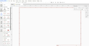
Figure 3. EasyEDA PCB Design Software Interface
For beginners, PCB design software with a user-friendly interface is essential. Popular design software include KiCad, Eagle, Altium, and EasyEDA… These programs allow you to create schematic diagrams, lay out components, and design circuit traces. You can also find standard component libraries to simplify the process. To keep the process simple, we use EasyEDA because of its huge online library and database.
Step 3: Create a schematic diagram when designing a circuit on EasyEDA
Once you have chosen the software, start by creating a schematic diagram. A schematic diagram is a blueprint of electrical connections, showing how components are connected. A PCB schematic can be created by looking at the component datasheet to arrange and connect the components accordingly.
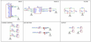
Figure 4. Schematic diagram of the circuit to be designed
Sometimes we need to change the value and type of components depending on the specific case. There are many different alternatives for a component. The schematic diagram in the IP2312 based charging module example attached above, the circuit is divided into different areas according to the function for the purpose of easy reading and reducing R&D time.
Step 4: Component layout on the board (PCB Layout)
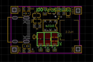
Figure 5. Component layout in PCB design
After creating the circuit diagram, the next step is to arrange the components on the PCB, including the following steps:
Determine the size of the circuit board.
Determine the location of the components to optimize performance and limit the length of the circuit.
Make sure the components are placed on the correct side, rotated in the correct direction, and aligned accurately.
Avoid overlapping components, and ensure sufficient distance for the soldering process.
In this example, all the components are placed close together to minimize the length of the circuit. Since we are designing the circuit for the IP2312 IC using the small circuit size of the TP4056 module, the reasonable arrangement of components plays an important role in the circuit routing.
Step 5: Wiring when designing a circuit on EasyEDA
Now comes the process of using circuit traces to connect the components. Traces are copper pathways that carry electrical signals between components. Use the following guidelines:
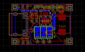
Figure 6. Connecting Components on a PCB
- Keep traces as short as possible to reduce resistance and noise.
- Route power and ground carefully, using wider traces for better performance.
- Pay attention to design rules, such as trace spacing, to avoid short circuits.
- Use through-holes to connect traces on different layers if necessary in multi-layer PCBs.
- Keep in mind the current rating and heat dissipation factor of the trace.
Online tools can be used to calculate the current rating for the traces. The design rules must be met, automated wiring can be used to reduce development time but be aware that this may not yield reliable results in some cases.
Step 6: Add Power Plane and Ground Plane
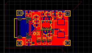
Figure 7. Grounding when designing a PCB on EasyEDA
For most printed circuits, especially those with high currents, adding a Power plane and Ground plane is very important. The Power plane conducts power evenly across the entire board, while the Ground plane reduces electrical noise. The Power plane and Ground plane are usually solid copper areas that cover the layers of the printed circuit.
The printed circuit in the example is designed with two layers, we added a Ground plane on both sides to reduce input voltage noise. The Ground plane is a pure copper layer added to the printed circuit and connects to all the GND pins of the components in the circuit.
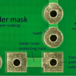
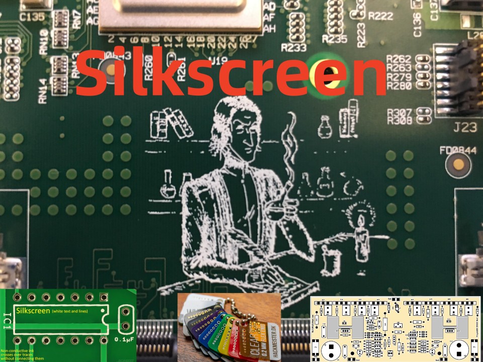
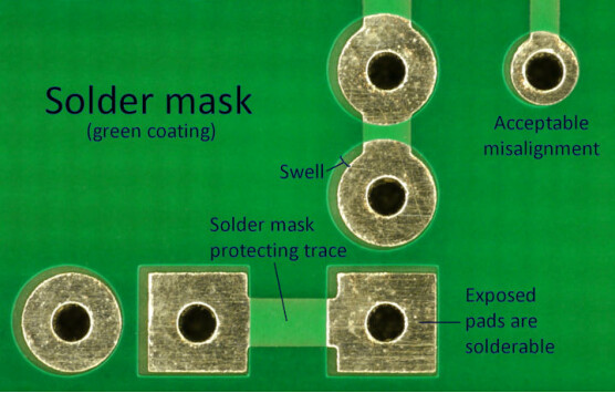
Step 7: Add names and symbols on the Silkscreen layer
Add Silkscreen for component codes, pin numbers, logos or regulatory markings. The Silkscreen layer is an important tool for assembly and troubleshooting, helping to identify components and their locations. It is important to ensure that the Silkscreen layer does not interfere with the solder joints or circuit traces. For more information, see our full article on the complete guide to Silkscreen on PCBs.
Figure 7. Information on the Silkscreen layer on the circuit design file
Step 8: Check the DRC design rules when designing the circuit on EasyEDA
Before finalizing the design, run the Design Rules Check (DRC) to detect any errors such as minimum spacing issues or unconnected traces. Most PCB design software includes a DRC tool, which helps ensure the design meets the manufacturer’s specifications without errors.
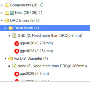
Figure 8. Error message after running DRC
Step 9: Export Gerber format processing files
Once your design is complete and verified, you need to export Gerber files. These files contain the information needed for manufacturers to fabricate the circuit. Each layer of your PCB (e.g. Top, Bottom, Silkscreen, Solder Mask) will be detailed in these files.
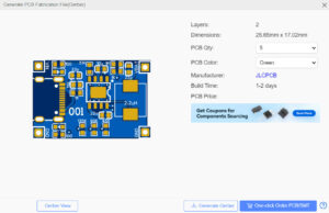
Figure 9. Exporting Gerber files on EASY EDA software
2. Advantages of designing circuits on EasyEDA
EasyEDA is a versatile tool for electronics engineers, enthusiasts and students, allowing for fast and efficient design, testing and verification of circuits. Its user-friendly interface and unique features have made it a popular choice.
Figure 10. Easy EDA software has both Online and Offline versions depending on user needs
Integration with other tools: EasyEDA supports many file formats such as Altium, Eagle, and KiCad, making importing/exporting designs seamless. It also integrates with cloud platforms such as Dropbox and Google Drive for easy project sharing and backup.
Low cost: EasyEDA is cost-effective, offering free options for small projects and affordable premium plans for advanced features.
3D visualization: With 3D visualization, users can view PCB designs in real time, helping to arrange components and identify potential design issues.
Schematic and PCB design: Users can design both schematics and PCBs in the same platform, with tools to import designs or create new designs from scratch.
Large component library: EasyEDA offers an extensive component library, including resistors, capacitors, transistors, and ICs. Users can also create or import custom components.
3. Conclusion
Finally, once you have your Gerber files, you can send them to your PCB manufacturer. Many manufacturers offer online quoting tools where you upload your files, choose your board specifications (like material and thickness), and place your order. Designing a printed circuit board may seem intimidating at first, but by following these steps, even beginners can design circuits that work well. Practice is key, and over time, you will develop the skills to optimize component placement, reduce noise, and create high-quality designs.
After completing the design file, you can send it directly to Hatakey Electronics to proceed with the order for printed circuit board processing according to the contact information below:
Sales 01: 0965 833 553
Email 01: hatakeyvn@gmail.com
Sales 02: 0927 277 222
Email 02: sales.hatakeyvn@gmail.com
Service feedback: 0971 687 227
Have fun designing!

 Tiếng Việt