
SILKSCREEN IN PCBA PROCESS
SILKSCREEN is used in PCB manufacturing technology to ensure the quality of the circuit board and the efficiency of assembly. The SILKSCREEN refers to the text and graphics characters printed on the PCB. They are used to identify the location, direction, and orientation of the components. In addition, the SILKSCREEN also provides manufacturing information for the PCBA process.
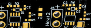
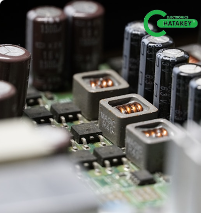
Figure 1: Lettering layer (SILKSCREEN) on PCB circuit
I. Importance
The lettering layer or SILKSCREEN layer is a necessary layer in the process of designing and manufacturing PCB circuits. They play a role in making it easy to assemble components on the surface of the circuit board. Mainly, they are soldered components or plug-in components to ensure accuracy and avoid errors. Therefore, specific and unified standards are needed to optimize the applications of the lettering layer.
II. Standards and applications
The following are the necessary standards and applications of the lettering layer (SILKSCREEN) on PCB circuits:
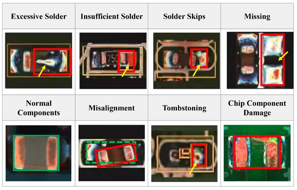
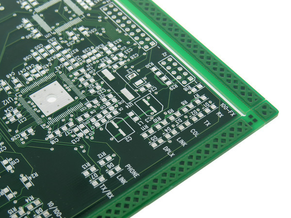
- Text layer displaying components, mounting holes and locating holes: For ease of installation and identification, all components, mounting holes and locating holes must have corresponding text layers. For example, mounting holes are numbered as H1, H2, etc. for ease of installation tracking to avoid errors.
- Text layer character direction: Characters must follow the rule from left to right and from bottom to top. This is to maintain visual consistency. In addition, for polarized components such as polarized capacitors and diodes, the direction must be consistent within the same type of component with the same function to reduce assembly errors.
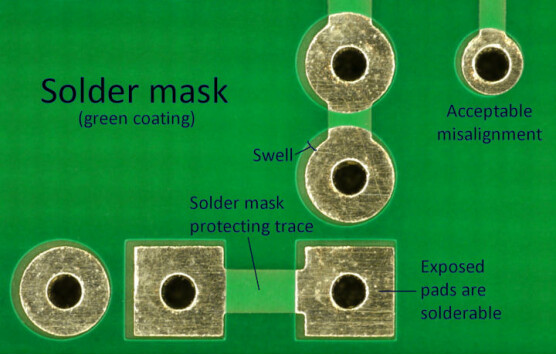
- Text layer display method for soldering pads and soldering lines: Text layers should not be used on the soldering pads of components and soldering lines to ensure the accuracy of the soldering process and the continuity of the soldering lines. In addition, the text layer should not be covered by installed components. This is to facilitate future repair and maintenance of the circuit.
- Lettering for Polarized Components: For polarized components such as capacitors and diodes, their polarity must be clearly marked on the lettering. This is for easy identification and to avoid incorrect installation.
- Connectors: The lettering for the connectors must indicate the correct mounting direction to avoid errors.
- Board name, date, version and other information: The lettering showing this information must be clearly visible. This is to aid in recording and identifying different versions of the PCB.
- Manufacturer information and ESD markings: The PCB must include the manufacturer information and ESD (Electrostatic Discharge) markings to indicate electrostatic discharge incidents for safety and compliance.
- Gerber file completeness: The Gerber file must include the necessary layers such as trace layer, lettering layer, solder mask layer, etc. . This is to ensure the accuracy of the manufacturing process.
- Symbol Consistency: The symbols on the PCB must be the same as the symbols in the BOM to ensure consistency between the two.
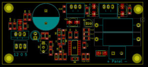
Figure 2: Application of SILKSCREEN layer.
III. Conclusion
The lettering design standards help ensure the correct identification and installation of components. To help increase assembly efficiency and reduce errors. Well-designed lettering symbols such as component name symbols, polarity and connection port orientation. This is essential for PCB assembly and maintenance. Correct lettering will avoid interference with soldering processes. In addition, it helps identify PCB versions and manufacturers. Compliance with these standards will improve the overall reliability and quality of PCBA, ensuring smooth production and maintenance processes.
If you have any questions, you can contact our HATAKEY Electronics company to have our experienced technical team with many years of experience in the industry answer all your questions. Hatakey.com.vn Electronics Company specializes in providing services related to PCB circuit boards such as ordering printed circuit boards with many different sizes and colors, processing and assembling circuits, designing circuit layouts, ordering electronic components from many reputable distributors. We can meet all the necessary needs of customers. Thank you for taking the time to read this article.
Some related articles:
FR4 – Material used in printed circuits
The reason why green is the main color in PCB manufacturing
Peeling of copper PAD during tin plating (HASL)
For more information, please contact:
Sales 01: 0965 833 553
Email 01: hatakeyvn@gmail.com
Sales 02: 0927 277 222
Email 02: sales.hatakeyvn@gmail.com
Service suggestions: 0971 687 227


 Tiếng Việt