
Component layout is an important task when designing printed circuit boards (PCBs), it significantly affects the performance, reliability and manufacturability of electronic devices. Reasonable component layout helps your board to have the best performance, limit noise and minimize risks related to overheating. In this article, Hatakey Electronics will discuss with you the options for component layout on the circuit, as well as things to pay attention to so that the board can achieve the best performance and ease in the assembly process.
1. What is component layout?
Component layout is the arrangement of electronic components on the printed circuit board. The stability and performance of the board depends a lot on this arrangement. Component layout with a suitable strategy will help manage heat effectively, reduce electromagnetic interference (EMI) and ensure signal integrity.
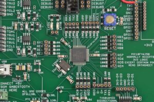
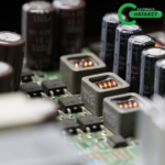
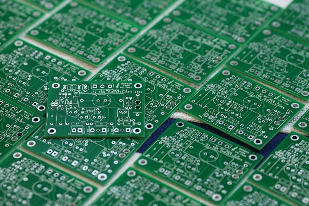
Figure 1. Component Layout on a PCB
2. Key Factors to Consider When Layouting Components on a PCB
Component Layout Near the Power Pin
One of the basic ideas of component layout is to place capacitors, resistors, and other important components near the power pins of ICs. The stable operation of a circuit depends on reducing noise and voltage fluctuations. Both of these can be achieved with proper component layout. Placing these components near the power pins reduces the length of the electrical path, thereby reducing impedance and improving the overall performance of the circuit.
Component Grouping
Another important element of good component layout is to group similar components together. Arranging resistors, capacitors, and inductors according to their purpose simplifies the PCB design and improves signal integrity. This reduces the risk of signal noise and streamlines the path of the electrical signal. Furthermore, proper grouping facilitates efficient manufacturing techniques and board layout.
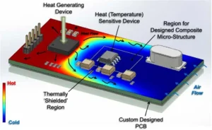
Thermal Management
Temperature control is critical for electronic components to operate within their ideal temperature range. Sufficient distance between components helps to minimize overheating and possible damage. Good temperature control not only improves component reliability but also improves the overall performance of the printed circuit board. Proper component layout, heat sinks, and heat sinks all help to control temperature properly.
3. The Importance of Component Layout in PCB Design
Ensuring Signal Integrity
Component layout is critical to maintaining signal accuracy. To minimize signal loss and noise, it is necessary to reduce the length of signal paths and avoid sharp bends. Good design techniques help ensure that signals traveling across the PCB are accurate and clear.
Mitigating EMI
Electromagnetic interference (EMI) can significantly affect the performance of electronic devices. Effective grounding and shielding provided by proper component layout and wiring can help reduce EMI. Ground planes and sensitive components located away from high-frequency signal paths can help reduce EMI issues.
Ensure Manufacturability
A properly laid-out board facilitates manufacturing, thereby reducing the likelihood of errors and failures during assembly. Automated assembly lines can mount and solder components more accurately depending on proper spacing and layout, thereby improving manufacturing efficiency and reducing costs.
Improve Reliability
The layout of a printed circuit board largely determines its reliability, helping to avoid mechanical stress, overheating, and electrical issues that can cause component failure. Correct spacing and alignment of components improves the overall lifespan and durability of the printed circuit board.
2. Some tips for effective component placement
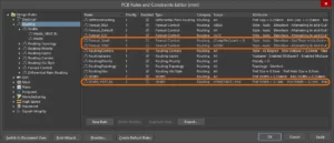
Check design rules
Modern printed circuit board design programs provide tools and features such as automatic wiring and real-time design rule checking to help with efficient component placement. Thanks to these tools, the design process can be simplified and compliance with component layout principles can be ensured.
Design Software
Design software follows specific design standards and rules for the PCB manufacturing process. These guidelines include trace width criteria, spacing restrictions, and other criteria that ensure the board operates consistently and meets industry standards.
Thermal Management
Regularly review the thermal management plan in your design. Make sure that heat-generating components are sufficiently spaced; consider using heatsinks and heat sinks if necessary.
Prototyping and Testing
Create prototypes and run extensive testing before deciding on the final PCB design. Before going into production, prototyping allows you to find and correct any layout errors, including hot spots or signal integrity issues.
3. Common Mistakes to Avoid When Layouting Components on a Circuit
Some common mistakes in the process of Layouting Components on a PCB can reduce performance and reliability. To achieve a high-quality design, it is necessary to be aware of and avoid these risks. Here are some common mistakes and solutions to avoid them.
Neglecting Signal Path Optimization
Neglecting signal path optimization is one of the most common mistakes. Signal paths that are too long and complex can cause noise, crosstalk, and delay, thereby reducing signal integrity. Especially for sensitive and high-frequency signals, keep signal paths short and straight to avoid problems. For high-speed signals, use differential signal pairs; in addition, use reasonable trace spacing to reduce noise.
Too many components
Putting too many components in a limited space can cause many manufacturing errors, thermal problems, and assembly problems. Poor air circulation due to dense components creates hot spots that can lead to reduced performance or damage to components. Ensuring that components are spaced properly helps dissipate heat, makes installation easier, and prevents problems. Proper component spacing also makes repairs and testing easier.
Improper Grounding
Improper grounding techniques can cause electromagnetic interference (EMI), signal interference, and unstable circuit operation. Not using a Ground Plane is a common mistake, while it is essential to reduce noise and ensure stable circuit operation. Avoid dividing the Ground Plane into discrete sections as this can lead to ground loops and EMI generation.
Decoupling Capacitor Placement
Maintaining a stable power supply voltage depends on decoupling capacitors, but sometimes they are placed too far away from the IC pins they are supposed to support. This increases the capacitance in the power rail, thus reducing the efficiency of the capacitor. To reduce capacitance and ensure stable operation, always place decoupling capacitors as close to the IC power pins as possible.
Poor thermal management
One of the main mistakes that can cause component failure and overheating is improper thermal management. Excessive heat can be caused by high power components being too close together or by not using heatsinks and heatsinks. Using heatsinks to transfer heat away from high heat dissipation areas and ensuring adequate spacing between components for heat dissipation helps prevent overheating.
Failure to follow DFM (Design for Manufacturing) principles
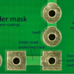
Ignoring DFM standards can lead to manufacturing issues including assembly errors, misplaced components, and poor solder joints. Consider trace width, pad size, and component orientation while always adhering to standard design rules. Work with your manufacturer early in your design to ensure your PCB can be manufactured properly and consistently.
Failure to consider power distribution
Improper power distribution can cause noise, voltage drop, and inefficient circuit operation. Make sure the trace is large enough to carry the required current; for complex designs, consider using multiple power planes. Maintaining stable voltage levels on a PCB depends on proper power distribution.
4. Conclusion
The success of electronic designs depends heavily on how components are arranged on the PCB. Always pay attention to placing necessary components near the power pins, grouping components and managing heat will help you build reliable and efficient printed circuits that meet current electronic needs. Accurate component placement ensures manufacturing and reliability, while improving signal integrity and reducing EMI, helping your designs succeed.
Hatakey Electronics hopes that the article can bring you useful information in component placement on PCB circuits. If you have any questions or need support when designing and manufacturing circuits, please contact us!
Sales 01: 0965 833 553
Email 01: hatakeyvn@gmail.com
Sales 02: 0927 277 222
Email 02: sales.hatakeyvn@gmail.com
Service suggestions: 0971 687 227


 Tiếng Việt